DESCRIPTION
2.8 inch wider view angle IPS TFT LCD module, with resolution 240x320 pixels. Portrait mode IPS TFT-LCD; this module is built in with ILI9341 controller IC; it supports MCU 8-bit/16-bit or SPI interface, contrast ratio 800 (typical value). It is a high brightness version, brightness 1000 nits (typical value). This 2.8” IPS TFT has a wider viewing angle than TN TFT, the view angle is Left:80 / Right:80 / Up:80 / Down:80 degree (typical value). The supply voltage for interface logic (IOVCC) of WF28J model is from 1.65V to 3.3V, supply for analog circuit is from 2.5V ~3.3V, normally black, transmissive LCD type, aspect ratio 3:4, glare surface glass. Operating temperatures from -20℃ to +70℃ and storage temperatures from -30℃ to +80℃.
DRAWING
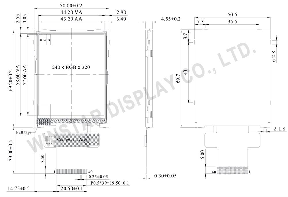
SPECIFICATIONS
Interface Pin Function
LCM PIN Definition
| NO | Symbol | Function | I/O |
|---|
| 1 |
GND |
Ground |
P |
| 2-6 |
NC |
No connection |
- |
| 7 |
VCI |
High voltage power supply for analog circuit blocks
(2.5 ~ 3.3 V) |
P |
| 8 |
IOVCC |
Low voltage power supply for interface logic circuits
(1.65 ~ 3.3 V) |
P |
| 9 |
TE |
Tearing effect output pin to synchronize MPU to frame writing, activated by S/W command. When this pin is not activated, this pin is low.
If not used, open this pin. |
O |
| 10 |
CS |
Chip select signal. |
I |
| 11 |
D/CX(SCL) |
(D/CX): This pin is used to select “Data or Command” in the parallel interface.
When DCX = 1, data is selected.
When DCX = 0, command is selected.
(SCL): This pin is used as the serial interface clock in 3-wire
9-bit/4-wire 8-bit serial data interface.
If not used, this pin should be connected to VDDI or VSS. |
I |
| 12 |
WR(SPI_D/C) |
(WRX) - 8080-Ⅰ/8080-Ⅱ system: Serves as a write signal and writes data at the rising edge.
(D/CX) - 4-line system: Serves as the selector of command or parameter.
Fix to VDDI level when not in use. |
I |
| 13 |
RD |
8080-Ⅰ/8080-Ⅱ system (RDX): Serves as a read signal and MCU read data at the rising edge.
Fix to VDDI level when not in use. |
I |
| 14-29 |
DB0~DB15 |
18-bit parallel bi-directional data bus for MCU system and RGB
interface mode
Fix to VSS level when not in use. |
I/O |
| 30 |
RESET |
This signal will reset the device and must be applied to properly initialize the chip.
Signal is active low. |
I |
| 31 |
IM0 |
Select the MCU interface mode
| IM2 | IM1 | 1M0 | MCU-Interface Mode | DB Pin in use |
|---|
| Register/Content | GRAM |
|---|
| 0 |
0 |
0 |
80 MCU 8-bit bus interface I |
D[7:0] |
D[7:0] |
| 0 |
0 |
1 |
80 MCU 16-bit bus interface I |
D[7:0] |
D[15:0] |
| 0 |
1 |
0 |
80 MCU 9-bit bus interface I |
D[7:0] |
D[8:0] |
| 0 |
1 |
1 |
80 MCU 18-bit bus interface I |
D[7:0] |
D[17:0] |
| 1 |
0 |
1 |
3-wire 9-bit data serial interface I |
SDA: In/Out |
| 1 |
1 |
0 |
4-wire 8-bit data serial interface I |
SDA: In/Out |
MPU Parallel interface bus and serial interface select
If use RGB Interface must select serial interface.
* : Fix this pin at VDDI or VSS. |
I |
| 32 |
IM1 |
| 33 |
IM2 |
| 34 |
DB16 |
18-bit parallel bi-directional data bus for MCU system and RGB
interface mode
Fix to VSS level when not in use. |
I/O |
| 35 |
DB17 |
| 36 |
LEDK |
Cathode of LED backlight. |
P |
| 37 |
LEDK |
Cathode of LED backlight. |
P |
| 38 |
LEDA |
Anode of LED backlight. |
P |
| 39 |
SDI(SDA) |
When IM[3] : Low, Serial in/out signal.
When IM[3] : High, Serial input signal.
The data is applied on the rising edge of the SCL signal.
If not used, fix this pin at VDDI or VSS. |
I/O |
| 40 |
SDO |
Serial output signal.
The data is outputted on the falling edge of the SCL signal.
If not used, open this pin |
O |
General Specifications
| Item | Dimension | Unit |
|---|
| Size |
2.8 |
inch |
| Dot Matrix |
240 x RGB x 320(TFT) |
dots |
| Module dimension |
50.5(W) x 69.7(H) x 4.55(D) |
mm |
| Active area |
43.2 x 57.6 |
mm |
| Dot pitch |
0.18 x 0.18 |
mm |
| LCD type |
TFT, Normally Black, Transmissive |
| TFT Driver IC |
ILI9341 or equivalent |
| TFT Interface |
MCU/SPI |
| Viewing angle |
80/80/80/80 |
| Aspect Ratio |
3:4 |
| Backlight Type |
LED,Normally White |
| Touch Panel |
Without Touch Panel |
| Surface |
Glare |
Absolute Maximum Ratings
| Item | Symbol | Min | Typ | Max | Unit |
|---|
| Operating Temperature |
TOP |
-20 |
- |
+70 |
℃ |
| Storage Temperature |
TST |
-30 |
- |
+80 |
℃ |
Electrical Characteristics
| Item | Symbol | Condition | Min | Typ | Max | Unit |
|---|
| Supply Voltage for digital |
IOVCC |
- |
1.65 |
- |
3.3 |
V |
| Supply Voltage for analog |
VCI |
- |
2.5 |
- |
3.3 |
V |
| Power Supply for Current |
ICC |
IOVCC=VCI
=VCC=3.28V |
- |
12 |
18 |
mA |
Specifiche di prodotto
|
Size
|
2.8" |
|
Resolution
|
240x320 |
|
Active Area (mm)
|
43.20x57.60 |
|
Color
|
Full Color |
|
Display Interface
|
MCU (Parallel/SPI) |
|
Display IC
|
ILI9341 |
|
View Angle
|
IPS |
|
Sunlight Readable
|
High 601~1200cd/m² |
|
Frame
|
No |
|
Touch Panel
|
No touch |
|
O. Temperature (°C)
|
-20~70 |
|
Data Connection
|
FPC for ZIF Connector |
|
Pin Nr.
|
40 |
|
Pin Pitch
|
0.5mm |
|
Preferred - Not Preferred
|
Preferred |