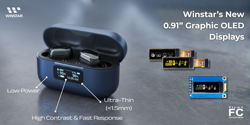
WEO16080W#AP3N00000-FC is a 1.54-inch COG graphic OLED display featuring a resolution of 160x80 dots. It measures 43.5 x 22.5 mm with an active area of 35.02 x 17.50 mm, and its slim profile of 1.41 mm is attributed to its COG structure.
Equipped with the SSD1320 IC, this module supports 6800/8080 8-bit, 4-wire SPI, and I2C interfaces. It offers 4-bit (16 Levels) grayscale and achieves an impressive contrast ratio of 10,000:1.
Operable with a logic power supply voltage ranging from 1.65V to 3.3V (typically 3.0V), the module operates reliably in temperatures from -40°C to +80°C, with a storage capability from -40°C to +85°C.
Ideal for a variety of applications including Networking Products, USB Testers, Smart Watches, Gaming Keyboards, and Smart Healthcare Devices such as oximeters and skin analyzers, WEO16080W#AP3N00000-FC enhances display quality with its crisp and vibrant screen.
With its high resolution (160x80 pixels) and low power consumption, this OLED display module is perfectly suited for performance-driven and efficient applications.