


I cookie ci aiutano a offrire i nostri servizi. Utilizzando i nostri servizi, acconsentite al nostro utilizzo dei cookie.
- Registrati
- Accesso
-
Carrello
(0)
Non ci sono articoli nel tuo carrello
Cerca
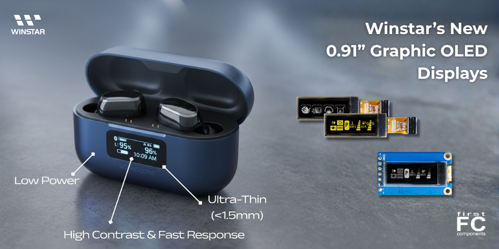
NT043-C003WS
Prodotti correlati
Ultimi prodotti visti