



Cerca
Filters
Close

WEO4864W#AP3N00F01-FC

PMOLED 0.71" Graphic 48x64, White color, COG, 3V, Interface I2C, Glare (FPC per Zif)

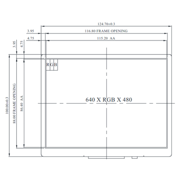
DRAWING

Winstar Display - 0.71" Graphic OLED 48x64, 0.71 oled


SPECIFICATIONS


Interface Pin Function

No.SymbolFunction
1 C2P Positive Terminal of the Flying Inverting Capacitorr Negative Terminal of the Flying Boost Capacitor The charge-pump capacitors are required between the terminals. They must be floated when the converter is not used.
2 C2N
3 C1P
4 C1N
5 VBAT Power Supply for DC/DC Converter Circuit
This is the power supply pin for the internal buffer of the DC/DC voltage converter. It must be connected to external source when the converter is used. It should be connected to VDD when the converter is not used.
6 NC No connection.
7 VSS Ground of Logic Circuit
This is a ground pin. It acts as a reference for the logic pins. It must be connected to external ground.
8 VDD Power Supply for Logic
This is a voltage supply pin. It must be connected to external source.
9 RES# Power Reset for Controller and Driver
This pin is reset signal input. When the pin is low, initialization of the chip is executed.
10 SCL The serial clock input
11 SDA The serial data input/output
12 IREF This is segment output current reference pin. 
When external IREF is used, a resistor should be connected between this pin and Vss to maintain the IREF current at a maximum of 30uA. 
When internal IREF is used, this pin should be kept NC
13 VCOMH Voltage Output High Level for COM Signal
This pin is the input pin for the voltage output high level for COM signals. A capacitor should be connected between this pin and VSS.
14 VCC Power Supply for OEL Panel
This is the most positive voltage supply pin of the chip. A stabilization capacitor should be connected between this pin and VSS when the converter is used. It must be connected to external source when the converter is not used.


Mechanical Data

ItemDimensionUnit
Dot Matrix 48 × 64 Dots
Module dimension 13.90 × 22.0 × 1.26 mm
Active Area 10.54 × 14.70 mm
Pixel Size 0.198 × 0.208 mm
Pixel Pitch 0.220 × 0.230 mm
Display Mode Passive Matrix
Display Color White
Drive Duty 1/64 Duty
IC SSD1306
Interface I2C
Size 0.71 inch


Absolute Maximum Ratings

ParameterSymbolMinMaxUnit
Supply Voltage for Logic VDD -0.3 4.0 V
Supply Voltage for Display VCC 0 15.0 V
Supply Voltage for DC/DC
(Internal DC/DC Enable)
VBAT -0.3 4.3 V
Operating Temperature TOP -40 +80 °C
Storage Temperature TSTG -40 +85 °C


Electronical Characteristics

ItemSymbolConditionMinTypMaxUnit
Supply Voltage for Logic VDD 1.65 3.0 3.3 V
Supply Voltage for Display
(Supplied Externally)
VCC 7.0 7.5 8.0 V
Charge Pump Regulator Supply Voltage VBAT - 3.0 - 4.2 V
Charge Pump Output voltage for Display (Generated by Internal DC/DC) Charge
Pump VCC
- 7.0 7.5 - V
Input High Volt. VIH 0.8 xVDD VDD V
Input Low Volt. VIL 0 0.2 xVDD V
Output High Volt. VOH 0.9 xVDD VDD V
Output Low Volt. VOL 0 0.1 xVDD V
Operating Current for VCC
(50% display ON)
(VCC Supplied Externally)
ICC - - 7 15 mA
50% Check Board operating Current
(VCC Generated by Internal DC/DC)
IBAT - - 15.0 25.0 mA


SKU: WEO4864W#AP3N00F01-FC
Brand: Winstar
Disponibile: No
Prezzi per quantità
Quantità
1+
5+
10+
25+
Prezzo
€6,50
€5,90
€5,50
€5,40

Per quantita’ maggiori di 25pz prego invii la richiesta a [email protected] o chiami il +39 0332 1888005

€6,50 IVA esclusa

DRAWING

Winstar Display - 0.71" Graphic OLED 48x64, 0.71 oled


SPECIFICATIONS


Interface Pin Function

No.SymbolFunction
1 C2P Positive Terminal of the Flying Inverting Capacitorr Negative Terminal of the Flying Boost Capacitor The charge-pump capacitors are required between the terminals. They must be floated when the converter is not used.
2 C2N
3 C1P
4 C1N
5 VBAT Power Supply for DC/DC Converter Circuit
This is the power supply pin for the internal buffer of the DC/DC voltage converter. It must be connected to external source when the converter is used. It should be connected to VDD when the converter is not used.
6 NC No connection.
7 VSS Ground of Logic Circuit
This is a ground pin. It acts as a reference for the logic pins. It must be connected to external ground.
8 VDD Power Supply for Logic
This is a voltage supply pin. It must be connected to external source.
9 RES# Power Reset for Controller and Driver
This pin is reset signal input. When the pin is low, initialization of the chip is executed.
10 SCL The serial clock input
11 SDA The serial data input/output
12 IREF This is segment output current reference pin. 
When external IREF is used, a resistor should be connected between this pin and Vss to maintain the IREF current at a maximum of 30uA. 
When internal IREF is used, this pin should be kept NC
13 VCOMH Voltage Output High Level for COM Signal
This pin is the input pin for the voltage output high level for COM signals. A capacitor should be connected between this pin and VSS.
14 VCC Power Supply for OEL Panel
This is the most positive voltage supply pin of the chip. A stabilization capacitor should be connected between this pin and VSS when the converter is used. It must be connected to external source when the converter is not used.


Mechanical Data

ItemDimensionUnit
Dot Matrix 48 × 64 Dots
Module dimension 13.90 × 22.0 × 1.26 mm
Active Area 10.54 × 14.70 mm
Pixel Size 0.198 × 0.208 mm
Pixel Pitch 0.220 × 0.230 mm
Display Mode Passive Matrix
Display Color White
Drive Duty 1/64 Duty
IC SSD1306
Interface I2C
Size 0.71 inch


Absolute Maximum Ratings

ParameterSymbolMinMaxUnit
Supply Voltage for Logic VDD -0.3 4.0 V
Supply Voltage for Display VCC 0 15.0 V
Supply Voltage for DC/DC
(Internal DC/DC Enable)
VBAT -0.3 4.3 V
Operating Temperature TOP -40 +80 °C
Storage Temperature TSTG -40 +85 °C


Electronical Characteristics

ItemSymbolConditionMinTypMaxUnit
Supply Voltage for Logic VDD 1.65 3.0 3.3 V
Supply Voltage for Display
(Supplied Externally)
VCC 7.0 7.5 8.0 V
Charge Pump Regulator Supply Voltage VBAT - 3.0 - 4.2 V
Charge Pump Output voltage for Display (Generated by Internal DC/DC) Charge
Pump VCC
- 7.0 7.5 - V
Input High Volt. VIH 0.8 xVDD VDD V
Input Low Volt. VIL 0 0.2 xVDD V
Output High Volt. VOH 0.9 xVDD VDD V
Output Low Volt. VOL 0 0.1 xVDD V
Operating Current for VCC
(50% display ON)
(VCC Supplied Externally)
ICC - - 7 15 mA
50% Check Board operating Current
(VCC Generated by Internal DC/DC)
IBAT - - 15.0 25.0 mA


Specifiche di prodotto
Brand Winstar
Size 0.71"
Risoluzione 48x64
Area Attiva (mm) 10.54x14.70
Dot Size 0.19x0.20
Polarizzatore Glare
Colore White
Alimentazione 3V
Interfaccia Display I2C
Display IC SSD1306
Struttura Costruttiva COG
Frame No
Touch Panel No touch
Temperatura O. (°C) -40~80
Connessione Display FPC for ZIF Connector
Nr. Pin 14
Passo Pin 0.5mm
Preferred - Not Preferred Preferred
Download
Specifiche di prodotto
Brand Winstar
Size 0.71"
Risoluzione 48x64
Area Attiva (mm) 10.54x14.70
Dot Size 0.19x0.20
Polarizzatore Glare
Colore White
Alimentazione 3V
Interfaccia Display I2C
Display IC SSD1306
Struttura Costruttiva COG
Frame No
Touch Panel No touch
Temperatura O. (°C) -40~80
Connessione Display FPC for ZIF Connector
Nr. Pin 14
Passo Pin 0.5mm
Preferred - Not Preferred Preferred