Search
Filters
Close

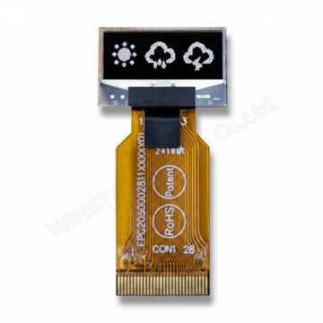
WEO9632W#CP3N00H00-FC

PMOLED 0.68" Graphic 96x32, White color, COG, 3V, Interface 6800,8080,SPI,I2C (FPC per Soldering), Glare

DRAWING


SPECIFICATIONS

Mechanical Data

ItemDimensionUnit
Dot Matrix 96 × 32 Dots
Module dimension 19.80 × 12.32 × 1.21 mm
Active Area 16.298 × 5.418 mm
Pixel Size 0.148 × 0.148 mm
Pixel Pitch 0.17 × 0.17 mm
Display Mode Passive Matrix
Display Color White
Drive Duty 1/32 Duty
IC SSD1315
Interface 6800, 8080,4-Wire SPI, I2C
Size 0.68 inch


Absolute Maximum Ratings

ParameterSymbolMinTyp.MaxUnit
Supply Voltage for Logic VDD -0.3 - 4 V
Supply Voltage for Display VCC 0 - 18 V
Operating Temperature TOP -40 - +80 °C
Storage Temperature TSTG -40 - +85 °C


Electronical Characteristics

DC Characteristics

ItemSymbolConditionMinTypMaxUnit
Supply Voltage for Logic VDD 1.65 3.0 3.3 V
Supply Voltage for Display VCC 7.5 12.0 12.5 V
High Level Input VIH 0.8×VDD VDD V
Low Level Input VIL 0 0.2×VDD V
High Level Output VOH Iout = 100uA 0.9×VDD VDD V
Low Level Output VOL Iout = 100uA 0 0.1×VDD V
Display 50% Pixel on ICC - 3.0 4.5 mA


Interface Pin Function

No.SymbolFunction
1 NC No connection
2 VSS Ground pin. It must be connected to external ground.
3 VCC Power supply for panel driving voltage. This is also the most positive power voltage supply pin. 
4 VCOMH COM signal deselected voltage level.
A capacitor should be connected between this pin and VSS.
5 IREF This is segment output current reference pin.
When external IREF is used, a resistor should be connected between this pin and VSS to maintain the IREF current at 30uA.
6 D7 These are 8-bit bi-directional data bus to be connected to the microprocessor’s data bus. When serial interface mode is selected, D0 will be the serial clock input: SCLK; D1 will be the serial data input: SDIN. When I2C mode is selected, D2, D1 should be tied together and serve as SDAout, SDAin in application and D0 is the serial clock input, SCL.
7 D6
8 D5
9 D4
10 D3
11 D2
12 D1
13 D0
14 E(RD#) This pin is MCU interface input.  When 6800 interface mode is selected, this pin will be used as the Enable (E) signal. Read/write operation is initiated when this pin is pulled HIGH and the chip is selected.  When 8080 interface mode is selected, this pin receives the Read (RD#) signal. Read operation is initiated when this pin is pulled LOW and the chip is selected.  When serial or I2C interface is selected, this pin must be connected to VSS.
15 R/W#
(WR#)
This is read / write control input pin connecting to the MCU interface.  When interfacing to a 6800-series microprocessor, this pin will be used as Read/Write (R/W#) selection input. Read mode will be carried out when this pin is pulled HIGH (i.e. connect to VDD) and write mode when LOW.  When 8080 interface mode is selected, this pin will be the Write (WR#) input. Data write operation is initiated when this pin is pulled LOW and the chip is selected.  When serial or I2C interface is selected, this pin must be connected to VSS.
16 D/C# This pin is Data/Command control pin connecting to the MCU.  When the pin is pulled HIGH, the data at D[7:0] will be interpreted as data.  When the pin is pulled LOW, the data at D[7:0] will be transferred to a command register.  In I2C mode, this pin acts as SA0 for slave address selection. 
17 RES# This pin is reset signal input. When the pin is pulled LOW, initialization of the chip is executed. Keep this pin HIGH (i.e. connect to VDD) during normal operation. 
18 CS# This pin is the chip select input connecting to the MCU.  The chip is enabled for MCU communication only when CS# is pulled LOW (active LOW). 
19 BS2 MCU bus interface selection pins. Select appropriate logic setting as described in the following table. BS2, BS1 are pin select
BS[2:1] Interface
00 4 lane SPI
01 I2C
11 8-bit 8080 parallel
10 8-bit 6800 parallel
Note
(1) 0 is connected to VSS
(2) 1 is connected to VDD 
20 BS1
21~22 VDD Power supply pin for core logic operation.
23 VSS Ground pin. It must be connected to external ground.
24 VCC Power supply for panel driving voltage. This is also the most positice power voltage supply pin.
25 NC No connection.
 
SKU: WEO9632W#CP3N00H00-FC
Brand: Winstar
Available: No
Price Breaks
Quantity
1+
5+
10+
25+
Price
€5.80
€5.30
€4.90
€4.80

For quantities above 25 pcs pls send your enquiry to [email protected] or call +39 0332 1888005

€5.80 excl tax

DRAWING


SPECIFICATIONS

Mechanical Data

ItemDimensionUnit
Dot Matrix 96 × 32 Dots
Module dimension 19.80 × 12.32 × 1.21 mm
Active Area 16.298 × 5.418 mm
Pixel Size 0.148 × 0.148 mm
Pixel Pitch 0.17 × 0.17 mm
Display Mode Passive Matrix
Display Color White
Drive Duty 1/32 Duty
IC SSD1315
Interface 6800, 8080,4-Wire SPI, I2C
Size 0.68 inch


Absolute Maximum Ratings

ParameterSymbolMinTyp.MaxUnit
Supply Voltage for Logic VDD -0.3 - 4 V
Supply Voltage for Display VCC 0 - 18 V
Operating Temperature TOP -40 - +80 °C
Storage Temperature TSTG -40 - +85 °C


Electronical Characteristics

DC Characteristics

ItemSymbolConditionMinTypMaxUnit
Supply Voltage for Logic VDD 1.65 3.0 3.3 V
Supply Voltage for Display VCC 7.5 12.0 12.5 V
High Level Input VIH 0.8×VDD VDD V
Low Level Input VIL 0 0.2×VDD V
High Level Output VOH Iout = 100uA 0.9×VDD VDD V
Low Level Output VOL Iout = 100uA 0 0.1×VDD V
Display 50% Pixel on ICC - 3.0 4.5 mA


Interface Pin Function

No.SymbolFunction
1 NC No connection
2 VSS Ground pin. It must be connected to external ground.
3 VCC Power supply for panel driving voltage. This is also the most positive power voltage supply pin. 
4 VCOMH COM signal deselected voltage level.
A capacitor should be connected between this pin and VSS.
5 IREF This is segment output current reference pin.
When external IREF is used, a resistor should be connected between this pin and VSS to maintain the IREF current at 30uA.
6 D7 These are 8-bit bi-directional data bus to be connected to the microprocessor’s data bus. When serial interface mode is selected, D0 will be the serial clock input: SCLK; D1 will be the serial data input: SDIN. When I2C mode is selected, D2, D1 should be tied together and serve as SDAout, SDAin in application and D0 is the serial clock input, SCL.
7 D6
8 D5
9 D4
10 D3
11 D2
12 D1
13 D0
14 E(RD#) This pin is MCU interface input.  When 6800 interface mode is selected, this pin will be used as the Enable (E) signal. Read/write operation is initiated when this pin is pulled HIGH and the chip is selected.  When 8080 interface mode is selected, this pin receives the Read (RD#) signal. Read operation is initiated when this pin is pulled LOW and the chip is selected.  When serial or I2C interface is selected, this pin must be connected to VSS.
15 R/W#
(WR#)
This is read / write control input pin connecting to the MCU interface.  When interfacing to a 6800-series microprocessor, this pin will be used as Read/Write (R/W#) selection input. Read mode will be carried out when this pin is pulled HIGH (i.e. connect to VDD) and write mode when LOW.  When 8080 interface mode is selected, this pin will be the Write (WR#) input. Data write operation is initiated when this pin is pulled LOW and the chip is selected.  When serial or I2C interface is selected, this pin must be connected to VSS.
16 D/C# This pin is Data/Command control pin connecting to the MCU.  When the pin is pulled HIGH, the data at D[7:0] will be interpreted as data.  When the pin is pulled LOW, the data at D[7:0] will be transferred to a command register.  In I2C mode, this pin acts as SA0 for slave address selection. 
17 RES# This pin is reset signal input. When the pin is pulled LOW, initialization of the chip is executed. Keep this pin HIGH (i.e. connect to VDD) during normal operation. 
18 CS# This pin is the chip select input connecting to the MCU.  The chip is enabled for MCU communication only when CS# is pulled LOW (active LOW). 
19 BS2 MCU bus interface selection pins. Select appropriate logic setting as described in the following table. BS2, BS1 are pin select
BS[2:1] Interface
00 4 lane SPI
01 I2C
11 8-bit 8080 parallel
10 8-bit 6800 parallel
Note
(1) 0 is connected to VSS
(2) 1 is connected to VDD 
20 BS1
21~22 VDD Power supply pin for core logic operation.
23 VSS Ground pin. It must be connected to external ground.
24 VCC Power supply for panel driving voltage. This is also the most positice power voltage supply pin.
25 NC No connection.
 
Products specifications
Brand Winstar
Size 0.68"
Resolution 96x32
Active Area (mm) 16.29x5.41
Dot Size 0.14x0.14
Polarizer Glare
Color White
Power supply 3V
Display Interface 6800/8080/SPI/I2C
Display IC SSD1315
Constructive Structure COG
Frame No
Touch Panel No touch
O. Temperature (°C) -40~80
Display Connection FPC for Soldering
Pin Nr. 25
Pin Pitch 0.65mm
Preferred - Not Preferred Preferred
Download
Products specifications
Brand Winstar
Size 0.68"
Resolution 96x32
Active Area (mm) 16.29x5.41
Dot Size 0.14x0.14
Polarizer Glare
Color White
Power supply 3V
Display Interface 6800/8080/SPI/I2C
Display IC SSD1315
Constructive Structure COG
Frame No
Touch Panel No touch
O. Temperature (°C) -40~80
Display Connection FPC for Soldering
Pin Nr. 25
Pin Pitch 0.65mm
Preferred - Not Preferred Preferred